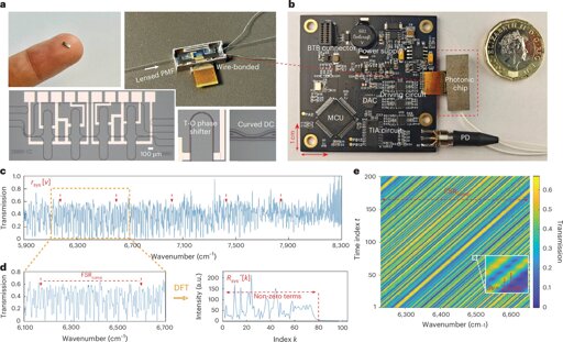
Researchers from the University of Cambridge and GlitterinTech, a startup founded by the same research group, have unveiled a fundamentally new type of optical spectrometer that delivers laboratory-grade precision in a device small enough to be embedded in portable and wearable technologies. By rethinking how spectra are measured and processed, the team has demonstrated a spectrometer costing only around $10, operating at a centimeter scale, and capable of applications ranging from industrial quality control to real-time health care monitoring.


Very cool!
I also like that they included a device cost analysis. I think they used some aggressively optimistic assumptions (100% yield from the wafer) and large-volume procurement prices that I am skeptical of, but if true it is valuable info.
Even at $50 a chip I could see applications for this.
Now I’m wondering, does the designer bear the cost of wafer yield, or the manufacturer?
Like do I pay for X amount of wafers and pray it’s got a good yield, or do I pay for Y amount of working chips and the manufacturer prays instead?
I feel like the manufacturer has the most impact on yield, but probably the contract provides an estimate for a specific process
I worked in contract manufacturing for making electronics.
We had certain contractual yields required. If the yield was below 90% (industry standard), they would pay us for the scrap. The assumption for that being they should have a confidence and reliability in their process that allows it to be higher. If we produced a higher yield than 90%, they got those for free.
Of course, yield numbers and reimbursement terms can be negotiated as part of the contracts.